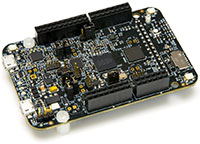
The Kinetis K27 and K28 USB ARM Cortex-M4 MCUs expand NXP's Kinetis K MCU portfolio with extra-large embedded memory of 2 MB Flash and 1 MB SRAM. They target applications which require processing efficiency as well as tight integration.
Highly integrated with two I2S interfaces, two USB controllers (high-speed with integrated high-speed PHY and full-speed crystal-less) and mainstream analog peripherals, the Kinetis K27 and K28 are also expandable through a 32-bit SDRAM memory controller and QuadSPI interface supporting eXecution-In-Place (XiP).
Kinetis K27 and K28 MCUs enable secure content using a true random number generator, cyclic redundancy check, memory mapped cryptographic acceleration unit, and provide a strong foundation to support requirements for the next generation of Internet of Things (IoT) applications.
Features
- Performance
- 150 MHz (max) ARM Cortex-M4 with DSP instructions and single precision floating point unit (FPU)
- 32-channel DMA with asynchronous support in stop mode.
- Cross bar switch enables concurrent multi-master bus accesses, increasing bus bandwidth
- Ultra-low-power
- Active run core power consumption @ 120 MHz: < 258 µA/MHz (TYP @ +25°C) for K28
- Static power consumption down to < 14 µA (TYP) with full 1 MB SRAM retention and < 6 µS wakeup
- Lowest static mode down to 454 nA (VLLS0) for K28
- Memory
- 2 MB dual bank embedded program Flash
- 1 MB of SRAM
- 8 KB I/D cache + 8 KB system cache
- 32-bit SDRAM controller
- QuadSPI interface with eXecution-in-Place (XiP)
- Mixed-signal capability
- 16-bit SAR ADC: Up to 18-ch single-ended / 3-ch differential
- 12-bit DAC
- Two analog comparators (CMP) containing a 6-bit DAC and programmable reference input
- 1.2 V analog voltage reference
- PMC with core voltage bypass (only K28)
- Timing and control
- One 4-ch periodic interrupt timer
- Two 16-bit low-power timer PWM modules
- Two 8-ch motor control/general purpose/PWM timers
- Two 2-ch quadrature decoder/general purpose timers
- Real-time clock with independent 3.6 V power domain
- Programmable delay block
- Connectivity and communications
- Dual USB controllers: high-speed (HS) with integrated HS PHY + crystal-less full-speed (FS) operations
- Five low power UART (LPUART) modules
- Two I2S modules for audio system interfacing and four I2C modules
- Four SPI modules (one supports up to 40 Mbps)
- 32-ch programmable module (FlexIO) to emulate various serial, parallel, or custom interfaces
- Secure digital host controller (SDHC)
- Reliability, safety, and security
- Cyclic redundancy check (CRC) engine validates memory contents and communication data, increasing system reliability
- True random number generator (TRNG)
- Memory mapped crypto acceleration unit (MMCAU): support DES, 3DES, AES, MD5, SHA-1, and SHA-256 algorithms
- Human-machine interface (HMI)
- 32-ch programmable module (FlexIO) to emulate various serial, parallel, or custom interfaces
Applications
- Wearable devices
- Mobile applications,IoT
- Low-end graphic display system
- Cost-optimized multi-standard wireless smart home hubs
- Home automation devices
- Consumer accessories
