TMS32C5517AZCHA20R

TMS32C5517AZCHA20R
Mfr. #:
TMS32C5517AZCHA20R
설명:
Digital Signal Processors & Controllers - DSP, DSC TMS320C5517 low-power digital signal processor 196-NFBGA -40 to 85
수명 주기:
이 제조업체의 새 제품입니다.
데이터 시트:
TMS32C5517AZCHA20R 데이터 시트
배달:
DHL FedEx Ups TNT EMS
지불:
T/T Paypal Visa MoneyGram Western Union
ECAD Model:
추가 정보:
TMS32C5517AZCHA20R 추가 정보 TMS32C5517AZCHA20R Product Details
제품 속성
속성 값
제조사:
텍사스 인스트루먼트
제품 카테고리:
디지털 신호 프로세서 및 컨트롤러 - DSP, DSC
RoHS:
Y
장착 스타일:
SMD/SMT
패키지/케이스:
NFBGA-196
시리즈:
TMS320C5517
제품:
DSP
핵심:
C55x
최대 클록 주파수:
75 MHz
데이터 RAM 크기:
64 kB, 256 kB
작동 공급 전압:
1.05 V
최소 작동 온도:
- 40 C
최대 작동 온도:
+ 85 C
상표:
텍사스 인스트루먼트
데이터 ROM 크기:
128 kB
인터페이스 유형:
I2C, SPI, UART, USB
데이터 버스 폭:
8 bit, 16 bit
입출력 전압:
1.8 V, 2.75 V, 3.3 V
지시 유형:
고정 소수점
습기에 민감한:
상품 유형:
DSP - 디지털 신호 프로세서 및 컨트롤러
공장 팩 수량:
1000
하위 카테고리:
임베디드 프로세서 및 컨트롤러
공급 전압 - 최대:
1.15 V
공급 전압 - 최소:
0.998 V
감시 타이머:
감시 타이머
Tags
TMS32C5, TMS32C, TMS32, TMS3, TMS
Service Guarantees

We guarantee 100% customer satisfaction.

Quality Guarantees

We provide 90-360 days warranty.

If the items you received were not in perfect quality, we would be responsible for your refund or replacement, but the items must be returned in their original condition.
Our experienced sales team and tech support team back our services to satisfy all our customers.

we buy and manage excess electronic components, including excess inventory identified for disposal.
Email us if you have excess stock to sell.

Email: [email protected]
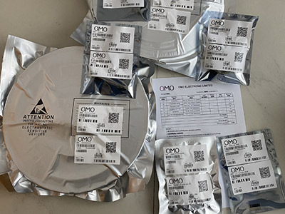
Step1: Vacuum Packaging with PL
Step1:
Vacuum Packaging with PL
Step2: Anti-Static Bag
Step2:
Anti-Static Bag
Step3: Packaging Boxes
Step3:
Packaging Boxes
***
This device is a member of TI's C5000 fixed-point Digital Signal Processor (DSP) product family and is designed for low active and standby power consumption.
***TEXAS
The device is based on the TMS320C55x DSP generation CPU processor core. The C55x DSP architecture achieves high performance and low power through increased parallelism and total focus on power savings. The CPU supports an internal bus structure that is composed of one program bus, one 32-bit data read bus and two 16-bit data read buses, two 16-bit data write buses, and additional buses dedicated to peripheral and DMA activity. These buses provide the ability to perform up to four 16-bit data reads and two 16-bit data writes in a single cycle. The device also includes four DMA controllers, each with 4 channels, providing data movement for 16 independent channel contexts without CPU intervention. Each DMA controller can perform one 32-bit data transfer per cycle, in parallel and independent of the CPU activity.
***XS
The C55x CPU provides two multiply-accumulate (MAC) units, each capable of 17-bit x 17-bit multiplication and a 32-bit add in a single cycle. A central 40-bit arithmetic and logic unit (ALU) is supported by an additional 16-bit ALU. Use of the ALUs is under instruction set control, providing the ability to optimize parallel activity and power consumption. These resources are managed in the Address Unit (AU) and Data Unit (DU) of the C55x CPU.
***AS INSTR
The C55x CPU supports a variable byte width instruction set for improved code density. The Instruction Unit (IU) performs 32-bit program fetches from internal or external memory and queues instructions for the Program Unit (PU). The PU decodes the instructions, directs tasks to the AU and DU resources, and manages the fully protected pipeline. Predictive branching capability avoids pipeline flushes on execution of conditional instructions.
***
The GPIO functions along with the 10-bit SAR ADC to provide sufficient pins for status, interrupts, and bit I/O for keyboards, and media interfaces.
***AS INSTR
Serial media is supported through two multimedia card and secure digital (MMC and SD) peripherals, three Inter-IC Sound (I2S Bus) modules, one serial port interface (SPI) with up to four chip selects, one master and slave multichannel serial port interface (McSPI) with up to three chip selects, one multichannel serial port (McBSP), one I2C multimaster and slave interface, and a universal asynchronous receiver/transmitter (UART) interface
***AS INSTR
The device peripheral set includes an external memory interface (EMIF) that provides glueless access to asynchronous memories, such as EPROM, NOR, NAND, and SRAM, as well as to high-speed, high-density memories such as synchronous DRAM (SDRAM) and mobile SDRAM (mSDRAM).
***NS
Additional peripherals include a configurable 16-bit universal host-port interface (UHPI), a high-speed universal serial bus (USB2.0) device mode only, a real-time clock (RTC), three general-purpose timers with one configurable as a watchdog timer, and an analog phase-locked loop (APLL) clock generator.
***AS INSTRU
The device also includes a tightly coupled FFT hardware accelerate that supports 8- to 1024-point (by power of 2) real- and complex-valued FFTs and three integrated LDOs to power different sections of the device, except CVDDRTC which requires an external power source: ANA_LDO to provide 1.3 V to the SAR and power-management circuits (VDDA_ANA), DSP_LDO to provide 1.3 or 1.05 V to the DSP core (CVDD), selectable on-the-fly by software as long as operating frequency ranges are observed, and USB_LDO to provide 1.3 V to the USB core digital (USB_VDD1P3) and PHY circuits (USB_VDDA1P3).
***NS
The device is supported by the industry’s award-winning eXpressDSP, Code Composer Studio Integrated Development Environment (IDE), DSP/BIOS, Texas Instruments’ algorithm standard, and a large third-party network. Code Composer Studio IDE features code generation tools including a C Compiler and Linker, RTDX, XDS100, XDS510, XDS560 emulation device drivers, and evaluation modules. The device is also supported by the C55x DSP library which features more than 50 foundational software kernels (FIR filters, IIR filters, FFTs, and various math functions) as well as chip support libraries.
TMS320C5517 Fixed-Point Digital Signal Processor
OMO Electronic TMS320C5517 Fixed-Point Digital Signal Processor (DSP) is based on the TMS320C55x DSP generation CPU processor core. The C55x DSP architecture achieves high performance and low power through increased parallelism and total focus on power savings. The CPU supports an internal bus structure that is composed of one program bus, one 32-bit data read bus and two 16-bit data read buses and two 16-bit data write buses. The device also has additional buses dedicated to peripheral and DMA activity. These buses provide the ability to perform up to four 16-bit data reads and two 16-bit data writes in a single cycle. The device also includes four DMA controllers, each with 4 channels, providing data movement for 16 independent channel contexts without CPU intervention. Each DMA controller can perform one 32-bit data transfer per cycle, in parallel and independent of the CPU activity.
Processors
OMO Electronic Processors provide a comprehensive portfolio, proven software, and worldwide support enabling industry-leading automotive and industrial solutions. TI is dedicated to advancing and optimizing today’s processors to meet tomorrow’s intelligence, performance and cost requirements in automotive and industrial applications. Scalable hardware and software platforms with common code allow designers to seamlessly reuse and migrate across devices to protect future investment.
영상 부분 # 설명
TMS32C5517AZCHA20R

Mfr.#: TMS32C5517AZCHA20R

OMO.#: OMO-TMS32C5517AZCHA20R

Digital Signal Processors & Controllers - DSP, DSC TMS320C5517 low-power digital signal processor 196-NFBGA -40 to 85
유효성
재고:
Available
주문 시:
1984
수량 입력:
TMS32C5517AZCHA20R의 현재 가격은 참고용이며 최상의 가격을 원하시면 판매팀 [email protected]으로 문의 또는 다이렉트 이메일을 보내주십시오.
참고 가격(USD)
수량
단가
내선 가격
1
US$10.73
US$10.73
10
US$9.87
US$98.70
25
US$9.36
US$234.00
100
US$8.34
US$834.00
250
US$7.93
US$1 982.50
500
US$7.42
US$3 710.00
1000
US$6.81
US$6 810.00
시작
최신 제품
Top