We guarantee 100% customer satisfaction.
Quality GuaranteesWe provide 90-360 days warranty.
If the items you received were not in perfect quality, we would be responsible for your refund or replacement, but the items must be returned in their original condition.
Our experienced sales team and tech support team back our services to satisfy all our customers.
we buy and manage excess electronic components, including excess inventory identified for disposal.
Email us if you have excess stock to sell.
Email: [email protected]

Very good product and service. Thank you
2019-04-18
Everything is fine. I did not check in the work. It came quickly.
2019-06-13| 부분 # | 설명 | 재고 | 가격 |
|---|---|---|---|
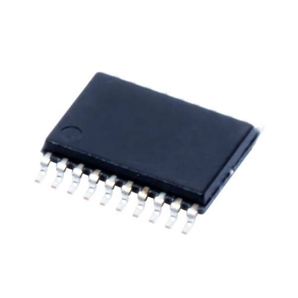
| TPS2311IPWR DISTI # V39:1801_07412610 | Hot Swap Controller 2-CH 5.5V/13V 20-Pin TSSOP T/R RoHS: Compliant | 0 | |
| TPS2311IPWR DISTI # TPS2311IPWR-ND | IC DUAL HOTSWAP PWR CONT 20TSSOP RoHS: Compliant Min Qty: 2000 Container: Tape & Reel (TR) | Temporarily Out of Stock |
|
| TPS2311IPWR DISTI # TPS2311IPWR | Hot Swap Controller 2-CH 5.5V/13V 20-Pin TSSOP T/R (Alt: TPS2311IPWR) RoHS: Compliant Min Qty: 2000 Container: Tape and Reel | Europe - 0 |
|
| TPS2311IPW DISTI # 595-TPS2311IPW | Hot Swap Voltage Controllers 3-13V Dual w/Intrdpt Chl Circuit Breaking RoHS: Compliant | 420 |
|
| TPS2311IPWR DISTI # 595-TPS2311IPWR | Hot Swap Voltage Controllers 3-13V Dual w/Intrdpt Chl Circuit Breaking RoHS: Compliant | 0 |
|
| TPS2311IPWG4 DISTI # 595-TPS2311IPWG4 | Hot Swap Voltage Controllers 3-13V Dual w/Intrdpt Chl Circuit Breaking RoHS: Compliant | 0 | |
| TPS2311IPWRG4 DISTI # 595-TPS2311IPWRG4 | Hot Swap Voltage Controllers 3-13V Dual w/Intrdpt Chl Circuit Breaking RoHS: Compliant | 0 |
| 영상 | 부분 # | 설명 |
|---|---|---|

|
Mfr.#: TPS2330EVM-184 |
TPS2330 Hot Swap Controller Evaluation Board |


