By Difference between PMOS and NMOS 6852
Core Principles and Structural Differences
Applications and Technology Progress
Performance Comparison and Selection Guide
Advantages and Disadvantages of NMOS and PMOS
In modern electronic technology, the Metal-Oxide-Semiconductor Field-Effect Transistor (MOSFET) is the basic unit of integrated circuits. Among them, the N-Channel MOS (NMOS) and P-Channel MOS (PMOS) are two main types. They support many semiconductor devices, from microprocessors to memory. Understanding their differences helps in circuit design and device selection. This text will analyze their features, working principles, and applications, and then compare them based on real technical needs.
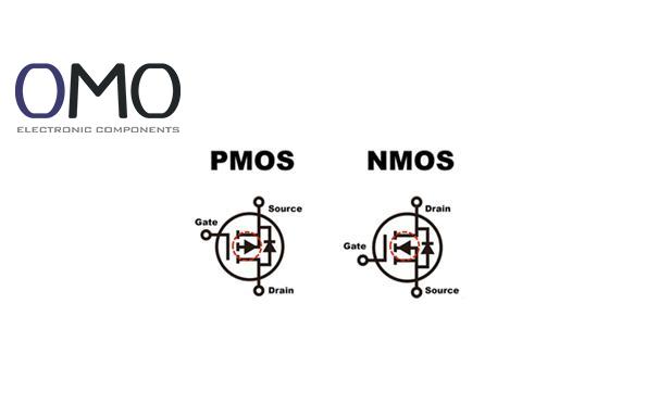
The NMOS (N-Channel Metal-Oxide-Semiconductor) transistor is a unipolar field-effect transistor that uses electrons as the majority carriers. It is a key part of modern digital circuits. Because of its high conductivity, it is often the first choice for high-performance integrated circuits.
An NMOS transistor uses the field effect to control current. The conductive channel is formed by electrons. Its typical structure includes:
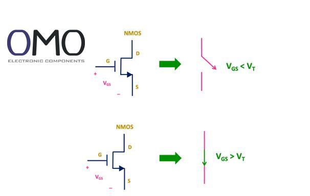
When the gate has enough positive voltage, an inversion layer forms under the gate, creating an electron channel.
Because electron mobility is high, NMOS has lower resistance and faster switching at the same size. Data shows that in a 0.18μm process, NMOS saturation current can be more than 2.5× that of PMOS of the same size. This makes NMOS better for high-speed uses. For example, in our new high-speed interface chip, NMOS drivers reach 5Gbps data transfer.
The PMOS transistor is the complementary type of NMOS. It uses holes as majority carriers. Although slower than NMOS, it has important roles in circuit design.
A PMOS is built in an N-type substrate or N-well. The source and drain are P+ doped regions. To turn it on, the gate must have a negative voltage, so a hole channel forms under the gate. Its structure is almost the same as NMOS, except for opposite doping.
Even with lower hole mobility, PMOS is valuable. For example, in our low-power power management chip, PMOS is used as a pull-up switch. In off-state, it has almost zero leakage current, reducing standby power to the microampere level.
| Feature | NMOS | PMOS |
| Substrate type | P-type silicon | N-type silicon / N-well |
| Source/Drain doping | N+ | P+ |
| Carrier type | Electrons | Holes |
This complementary behavior is the base of CMOS (Complementary MOS) technology. For example, in our smart power module, NMOS handles large current pull-down, and PMOS manages power pull-up. This increases efficiency by more than 30%.
The Body Effect means the threshold voltage changes when the source-to-body voltage (V_SB) changes.
Designers must consider this. For example, in our high-precision analog chip, special well isolation reduces body effect to 1/3 of traditional designs, keeping switching stable at different voltages.
Old NMOS/PMOS-only logic had high power use and low noise margin. It is no longer used.
CMOS uses both NMOS and PMOS:
In our next-generation IoT chip, we use an optimized CMOS design: NMOS for speed-critical paths, PMOS for power management. This lowers power by 40% while keeping performance.
| Feature | NMOS | PMOS |
| Carrier mobility | High (≈600 cm²/V·s) | Low (≈250 cm²/V·s) |
| Switching speed | Fast | Slow |
| Drive strength | Strong | Weak |
| Size for same current | Small | Large (2–3× width) |
| Static power | Exists | Exists |
| Integration density | High | Low |
High electron mobility → faster speed and better performance.
Higher drive current at the same size.
Alone (like NMOS logic), it has static power when output is low.
More sensitive to body bias effect.
Simpler manufacturing process (historically).
Works well as pull-up in CMOS, perfectly complements NMOS.
Lower hole mobility → slower speed and weaker drive.
Needs larger size (width) to match NMOS drive, using more chip area.
NMOS transistors, defined by their N-type channel, operate using electrons as the majority charge carriers. In contrast, PMOS transistors, which have a P-type channel, rely on the movement of holes for operation.
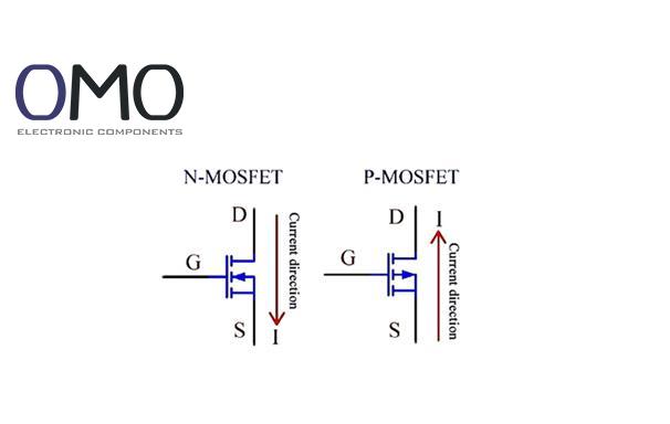
NMOS and PMOS transistors team up in CMOS pairs to form logic gates and circuits. The NMOS pulls down the output when active, while the PMOS pulls it up.
A PMOS transistor, which stands for P-Channel Metal-Oxide-Semiconductor, is a type of MOSFET. Its operation relies on the flow of holes. The device switches to its 'on' state upon the application of a negative voltage at its gate terminal relative to the source, enabling current flow.
NMOS offers higher electron mobility, leading to faster switching and lower on-resistance. This makes it more efficient for high-speed digital applications.